The Strategic Emphasis on Advanced Chip Packaging by a Leading Semiconductor Firm
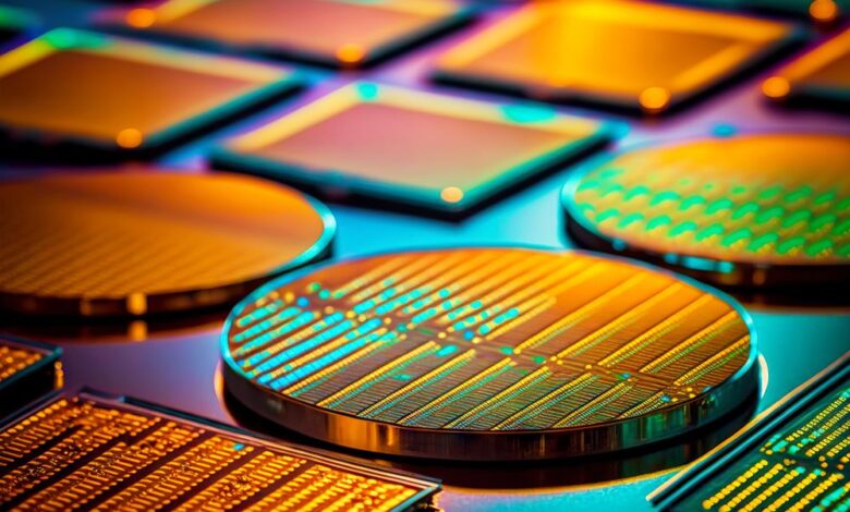
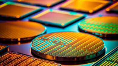
In the dynamic realm of semiconductor technology, a notable shift is taking place, with advanced chip packaging becoming a pivotal area of focus. A leading semiconductor enterprise is making significant strides in this domain, aiming to cater to the burgeoning demand for high-bandwidth memory (HBM), which is crucial for artificial intelligence (AI) advancements. This firm’s strategic investment and innovation in chip packaging underscore its commitment to maintaining a competitive edge in the AI memory market.
The semiconductor industry is witnessing a transformation as enterprises like this one channel over $1 billion into enhancing the final stages of chip production in South Korea. The move is a calculated effort to bolster power efficiency and performance, securing a dominant position in the HBM market. The enterprise’s shift from front-end chip design to back-end processes such as packaging is a response to the requirements of modern AI, which necessitates the swift handling of extensive data sets.
The firm’s advanced packaging techniques have not gone unnoticed, earning the trust of industry giants to supply HBM for AI accelerators. This collaboration has been a boon, contributing to the corporation’s substantial growth and elevating its market value significantly. The expertise of key figures in the organization, particularly in 3D integration technology, has been a cornerstone of this success. Their pioneering work in Through-Silicon Via (TSV)-based 3D packaging technologies has laid a solid foundation for the development of HBM, enabling the vertical stacking of chips and their interconnection through TSVs for enhanced data processing efficiency.
The journey of this semiconductor enterprise with HBM dates back to 2013, marking the beginning of its influence in the market through a partnership with a US-based technology company. The introduction of HBM technology remained unchallenged for a considerable period until competitors emerged. With the addition of seasoned experts to the team in 2018, the firm has fortified its advancements in HBM technology, reflecting a broader industry trend that prioritizes efficient and powerful memory solutions for AI development.
The strategic focus on advanced chip packaging and the enhancement of HBM technology by this semiconductor firm highlights its unwavering dedication to innovation and leadership in the AI memory market. The progress achieved in this field not only showcases the firm’s technical prowess but also its capacity to evolve with the changing demands of the semiconductor industry. As the firm advances, it plays a crucial role in shaping the technological infrastructure that will power the next generation of AI applications.
Source link